


Shenzhen Senyan Circuit Co., Ltd.
- Annual Revenue >1000000 USD
- Employees >100
- Year Established 2017
- Manufacturer, Distributor/Wholesaler, Exporter, Other


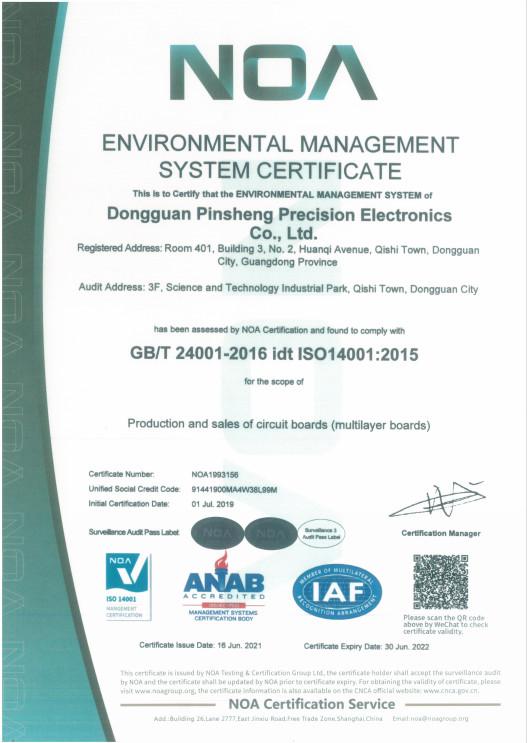
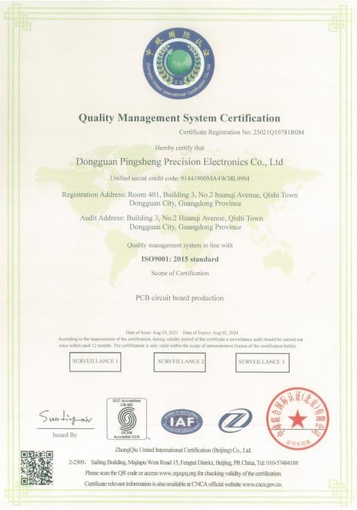
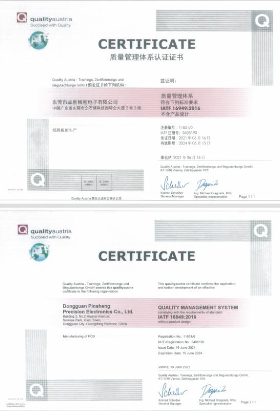
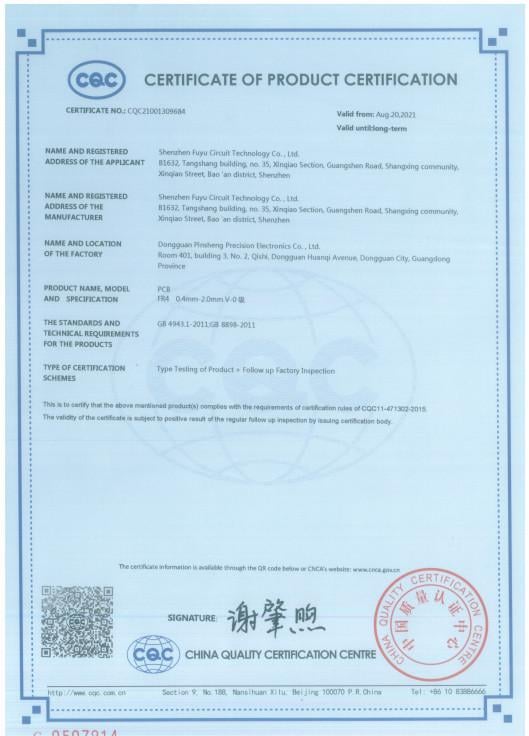
Certification
See All


 Copyright 2023 ucbis.com All Rights Reserved.
FR4 94v0 PCBA Manufacturing RoHS Electronic ISO9001
Pcba Manufactures Electronic Services PCBA Ru 94v0 Rohs Printed Circuit Board Assembly Manufacturer PCB
- Place of Origin: China (Mainland)
- Brand Name: SENYAN
- Base Material: FR-4
- Copper Thickness: 1oz
- Board Thickness: 1.6mm
- Min. Hole Size: 0.1mm
- Min. Line Width: 4mil
- Min. Line Spacing: 4mil
- Surface Finishing: HASL lead free
Welcome To Senyan.
Senyan is a PCB manufacturer, Senyan‘s capable of providing turn-key and partial turn-key printed circuit board assembly services.
For full turn-key, we take care of the entire process, including manufacturing of Printed Circuit Boards, procurement of components (100% original) , PCBA Testing , continuous monitoring of quality and final assembly.
Our main service:
1. PCB development and design;
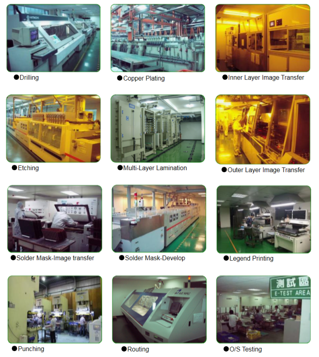
2. PCB manufacturing from 1 to 32 layers(Rigid PCB,Flexible PCB,Ceramci PCB,Aluminum PCB);
3. PCB Clone;
4. Component sourcing;
5. PCB Assembly;
6. Write program for customers;
7. PCB/ PCBA Test.
Flexible Volume Assembly Alternatives:
Prototype PCB Assembly
Low-Volume, High Mix PCB Assembly
High-Volume PCB Assembly
Consigned & Partial PCB Assembly
Full Turnkey PCB Assembly
Cable & Wire Harness Assembly
Box Build Assembly Services
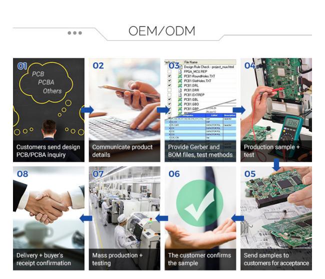
*PCB or PCBA Files Requests
1. Gerber files of the bare PCB board
2. BOM (Bill of material) for assembly (To short the lead time, please kindly advise us if there is any acceptable components substitution.)
3. Testing Guide & Test Fixtures if necessary
4. Programming files & Programming tool if necessary
5. Schematic if necessary
|
Your Troubles
|
|
Our Strategy
|
||
|
Lack of engineering experience
Various unexpected problems, causing the project to fail
|
|
Rich engineering experience: Bom Engineer/ Product Engineer/ Technical Engineer /Purchasing Engineer.Eliminate Problems and pitfalls at the design stage
|
||
|
Coordinating multiple suppliers
Insufficient time and energy
|
|
PCB Assembly and welding factory, Component procurement team,Function Test , Finished Product Assembly. Provide one-stop service, save time and worry
|
||
|
Product quality control
High hardware trial and error cost
|
|
Rigorous process and strong strength
We have established a standardized and rigorous process and system to effectively reduce quality problems
|
||
|
Traders do not have physical factories
The quality is not guaranteed, Documents easy to disclose
|
|
Own teams and factory, the delivery time is more controllable
|
||
|
Hard delivery guarantee
The market can't wait
|
|
Complete Organizational Structure: Project Department, Engineering Department, Purchasing Department, Quality Department,
Production Department, Etc. |
||
Why Choose Us
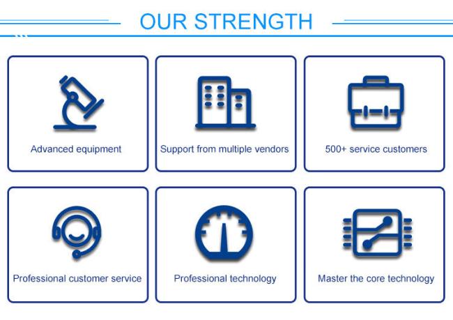
1. Fast response;
2. Lower cost;
3. Two-year guarantee.
With more than 10-year EMS service experience, we have established good businedd relationship with components manufacturers, and distributors. As we are sourcing these components together, which will benefit to get a good price from manufacturers.
The raw material in low price makes your own products more competitive in your market, in the meantime you can get 2 years guarantee with no worries from us; That is why we can keep good quality and competitive prices for global valued customers.
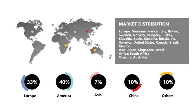
Senyan is a professional double sided PCB manufacturer.we produce varieties of 4layers sided PCB that include FR4 base material, polyimide base material,Metal base material, copper base material.products are sold to America,Uk,Germany,France,Italy,Belgium,Japan, Russian,Spanish,India,Hungary,Brazil and Korea etc.
Detailed for Pcb Assembly
Technical requirement:
1) Professional Surface-mounting and Through-hole soldering Technolog
2) Various sizes like 1206,0805,0603 components SMT technology
3) ICT(In Circuit Test),FCT(Functional Circuit Test) technology.
4) PCB Assembly With UL,CE,FCC,Rohs Approval
5) Nitrogen gas reflow soldering technology for SMT.
6) High Standard SMT&Solder Assembly Line
7) High density interconnected board placement technology capacity
With Large Monthly Production Capacity
With the help of our 15 CAM engineers, 15 SMT machine engineers and 10 BOM analysis engineers, our PCB production capacity can reach 40,000 square meters and EMS assembly capacity at 150 million components per month. Moreover, our reliable world-famous brand component procurements are as follows:
Global procurement database
Distribution partnership
Flexible stocking programs
Integrated customer registered pricing
Extensive global supply chain
OEM sourcing agreements
|
SMT Manufacturing Capability
|
|||
|
Item
|
Manufacturing Capability in process
|
Manufacturing Method
|
|
|
Production size(Min/Max)
|
50×50mm / 500×500mm
|
|
|
|
Production board thickness
|
0.2 ~ 4mm
|
|
|
|
Printing solder paste
|
Support method
|
|
Magnetism fixture, vacuo platform
|
|
|
|
Sticking up by vacuo, clamping on both sides ,flexible clamping with sheet, flexible clamping with thick board
|
|
|
Cleaning Method of printing solder paste
|
|
Dry method+ wetting method+ Vacuo method
|
|
|
Accuracy of printing
|
±0.025mm
|
|
|
|
SPI
|
Repeated accuracy of volume
|
<1% at 3σ
|
|
|
Mounting component
|
Components size
|
0603(Option) L75mm Connector
|
|
|
Pitch
|
0.15mm
|
|
|
|
Repeated accuracy
|
±0.01mm
|
|
|
|
AOI
|
FOV size
|
61×45mm
|
|
|
Test speed
|
9150mm²/Sec
|
|
|
|
3D X-ray
|
Shootingangle
|
0-45
|
|
Detail For PCB:
|
Item
|
Capability
|
|
1.Base Material
|
FR-4 / High TG FR-4 /Aluminum /CEM-1/Rogers/Arlon/Taconic/Teflon
|
|
2.Layers
|
1-22
|
|
3.Finised inner/outer copper thickness
|
1-6OZ
|
|
4.Finished board thickness
|
0.2-7.0mm
|
|
5.Min hole size
|
Mechanical hole: 0.15mm Laser hole: 0.1mm
|
|
6.Controlled Impedance
|
+/-5%
|
|
7.Plugging vias capability
|
0.2-0.8mm
|
|
8.Outline profile
|
Rout/ V-cut/ Bridge/ Stamp hole
|
|
9.Surface treatment
|
HASL, HASL lead free, Immersion Gold, Immersion Tin, Immersion Silver, Hard gold, Flash gold, OSP…
|


Q1. What is needed for PCB/PCBA quotation?
A:PCB : Quantity, Gerber file and Technical requirements (material,board thickness,, copper thickness,surface finish treatment...)
PCBA: PCB information, BOM, (Testing documents...)
Q2. What file formats are accepted for bare board PCB fabrication?
A:Gerber formats RS274X and RS274D are preferred. The Gerber RS274D format will require a separate aperture list for each file.Depending on the complexity, we may also accept design files in ODB++ and DWG file formats.
Q3. Are my files safe?
A:Your files are held in complete safety and security.We protect the intellectual property for our customers in the whole process..All documents from customers are never shared with any third parties.
Q4. MOQ?
A:No MOQ.
Q5.Shipping cost?
A:The shipping cost is determined by the destination, weight, packing size of the goods. Please let us know if you need us to quote you the shipping cost.
Q6.Can I have multiple orders shipped in one pachage?
A:Yes. Shipping multiple orders in one package will reduce your shipping costs. When placing your order through a sales rep,they'll automatically do their best to combine shipments when possible.
Q7. How do I track my order.
A: Your sales representative will provide tracking once your order has shipped.
Q8. How do I count the lead time?
A: The lead time schedule is as follows:
| 3 Day Lead Time | 4 Day Lead Time | 5 Day Lead Time | |||||
| Order Date | Ship Date | Order Date | Ship Date | Order Date | Ship Date | ||
| Monday | Thursday | Monday | Friday | Monday | Next Monday | ||
| Tuesday | Friday | Tuesday | Next Monday | Tuesday | Next Tuesday | ||
| Wednesday | Next Monday | Wednesday | Next Tuesday | Wednesday | Next Wednesday | ||
| Thursday | Next Tuesday | Thursday | Next Wednesday | Thursday | Next Thursday | ||
| Friday | Next Wednesday | Friday | Next Thursday | Friday | Next Friday | ||
Below is our standard lead time matrix which we can offer in normal circumstances. Please contact our team to confirm if we can meet your lead time.
| Order Type | Size (sq/m) | Best Lead Time (WDS) | Standard Lead Time (WDS) |
| NPI/Prototype | 0 – 1 | 1, 3, 5, 7 | 15 |
| HMLV (High Mix Low Volume) | 1 – 15 | 5, 7, 10 | 15 |
| Production – Small | 15 – 100 | 5, 7, 10 | 15 – 20 |
| Production – Medium | 100 – 300 | 7, 10 | 18 – 25 |
| Production – High | >300 | 15 | 25 – 30 |
All lead times are in manufacturing working days (WDS) and do not consider freight. Actual lead times might vary based on the availability of raw material and the specifications of the part. Due to the production cycle times, not all technologies can achieve the presented WDS.